中文 (中国)
 Tiếng Việt
 한국어
한국어
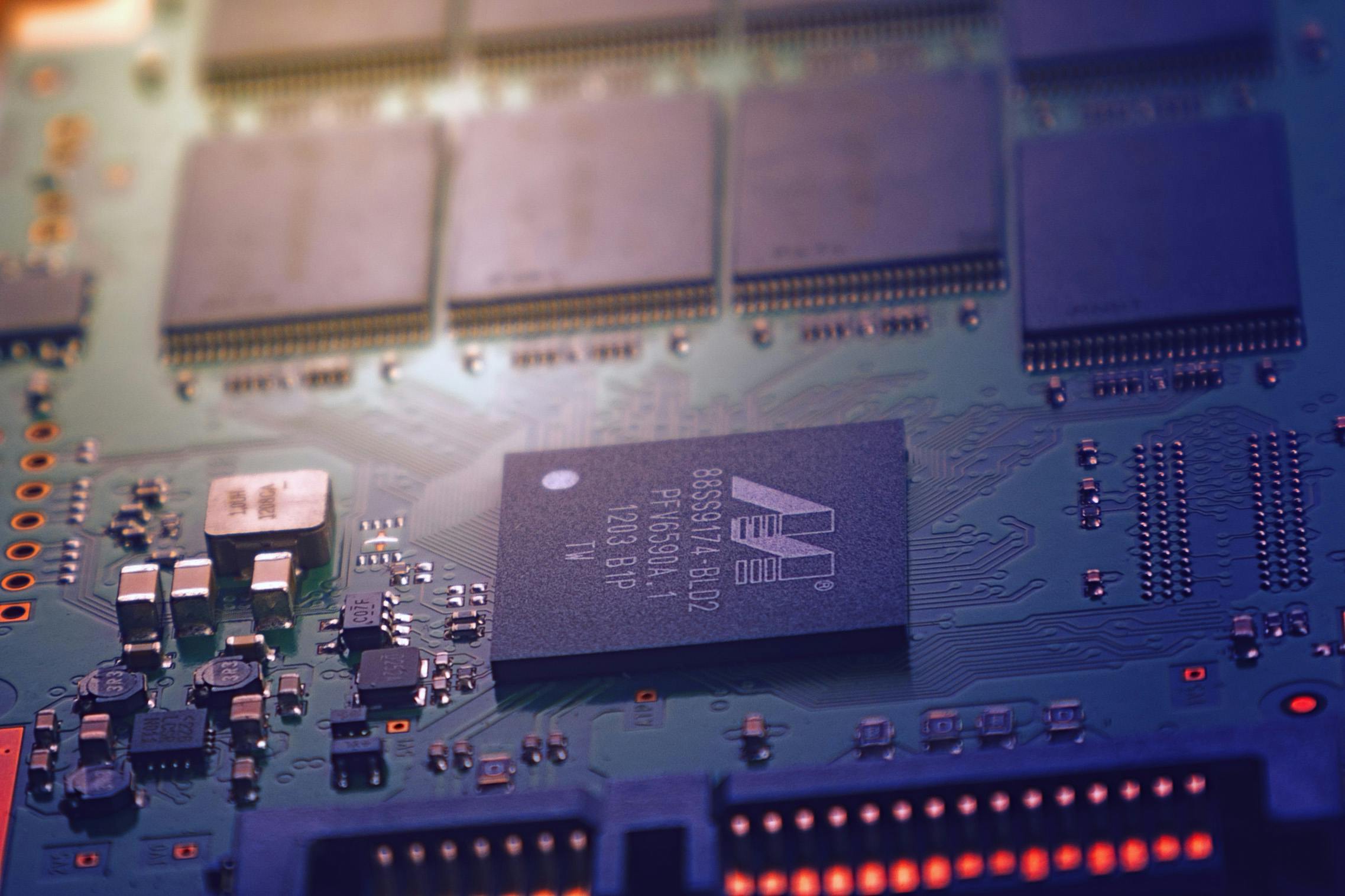
Plasma Surface Treatment machines are becoming a crucial technology in the semiconductor industry thanks to their highly effective deep cleaning and surface modification capabilities. This method helps remove impurities and metal oxides while simultaneously increasing surface energy to improve adhesion in manufacturing processes. With plasma, stages such as wire bonding, coating, painting, or chip packaging are optimized, limiting NSOP defects and enhancing product reliability. This is the pioneering solution for the sustainable development of the modern microchip industry.
1. Introduction to Plasma Treatment Technology
Plasma surface treatment machines are creating breakthroughs in many industrial fields. This technology uses ionized gas to remove impurities, modify surface characteristics, and create optimal conditions for bonding processes. In the semiconductor industry, plasma plays a vital role in the manufacturing and development of devices such as integrated circuits (ICs), MEMS, and nano-components.
What is plasma treatment technology?
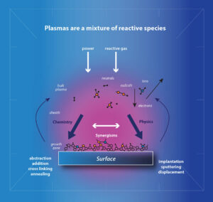
Plasma treatment technology is the process of using ionized gas to act upon a material to remove impurities or alter its surface characteristics. This is not just a cleaning stage, but also combines surface modification and material etching.
Common applications of plasma surface treatment machines include:
- Decontaminating contact surfaces
- Increasing surface roughness
- Increasing surface energy
- Creating hydrophilic or hydrophobic surfaces
- Removing metal oxides through physical and chemical interactions
Consequently, plasma plays an important role in enhancing adhesion and ensuring product quality.
2. Main Applications of Plasma in Industry
- Surface cleaning:
- Plasma machines use high-energy ions and active molecules to effectively remove organic, inorganic impurities, and residues.
- The result is a pure, defect-free surface that meets the strict standards of microchip and electronic component manufacturing.
- This is an important step to ensure precision and limit defects in subsequent stages.
- Surface activation:
- Plasma helps increase surface energy, thereby significantly improving adhesion.
- Applied in many stages such as bonding, painting, printing, or coating, where a strong bond between material layers is required.
- Thanks to surface activation, products achieve higher quality, and their durability and lifespan are markedly increased.
- Surface coating:
- Plasma technology allows the creation of thin, uniform coatings with strong adhesion.
- This coating protects the material against mechanical, chemical, and environmental impacts.
- As a result, the material is wear-resistant, corrosion-resistant, enhancing its lifespan and reducing maintenance costs.
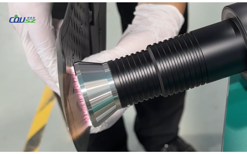
3. Applications of Plasma Surface Treatment Machines in the Semiconductor Industry
In semiconductor manufacturing, plasma machines are applied in many critical stages such as:
3.1. Cleaning and increasing wire bonding efficiency
Before performing wire bonding, the lead frame and chip are cleaned with plasma to increase the successful connection rate. This process also prevents voiding and delamination during molding, helping to improve packaging productivity.
Specifically, plasma helps resolve NSOP (Non Stick on Pad) defects – when the wire fails to bond to the chip pad due to surface oxidation or contamination.
3.2. Surface preparation before packaging
In the wire bonding process, surface preparation is a key factor. Plasma completely removes impurities, activates the surface, and ensures the metal wire bonds firmly to the chip pad. This reduces deviations, and increases the reliability and lifespan of semiconductor components.
3.3. Solving NSOP defects with Ar/H2 plasma
An experiment showed that gold-palladium coated pads often encounter NSOP due to surface oxides. When using Ar/H2 plasma, the active hydrogen reacts with the oxide and quickly removes it. As a result, NSOP defects drop sharply, and wire bonding efficiency increases significantly.
3.4. Enhancing bondability
Plasma machines help remove organic impurities and residual metal oxides from previous stages like die attach or snap curing. Consequently, the pull and shear strength of wire bonds are markedly improved, increasing bond durability and stability. This translates to higher productivity and better profits for businesses.
4. Outstanding Benefits of Plasma in the Semiconductor Industry
- Precise control, creating intricate patterns for semiconductor chips
- Ensures absolute cleanliness, minimizing defects
- Increases the reliability and lifespan of semiconductor devices
- Delivers high production efficiency, boosting ROI for businesses
Conclusion
Plasma coating machines are reshaping the semiconductor industry due to their precise cleaning, surface modification, and etching capabilities. This technology helps prevent NSOP defects, increases wire bonding efficiency, and ensures semiconductor chip quality. In the context of ever-growing microchip demand, plasma is the pioneering technological solution, promising an efficient and sustainable future.
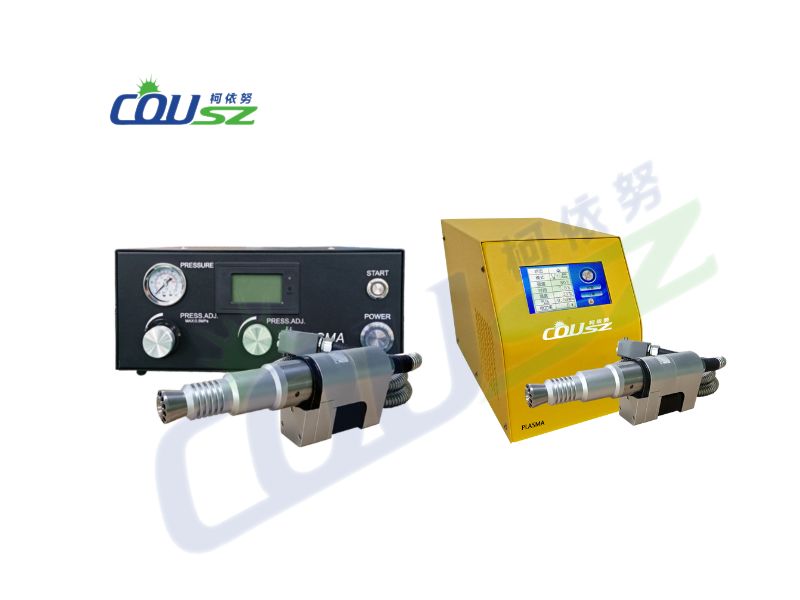
5. Why Choose COUSZ Brand Plasma Coating Machines?
The COUSZ brand has affirmed its position in the market with high-quality Plasma coating machines, optimal designs, and competitive prices. Some highlights include:
- Stable quality, high durability
- Free consultation on machine selection, tailored to actual production needs
- Clear warranty, fast technical support
Do not hesitate to contact us today to receive a free technical consultation and a special quote from our team of experts.
 Hotline: 0965 535 348 (Ms. Yuna / Ms. Hina)
 Email: sales03@cousz.com
 Website: https://cousz-vn.com/ |
 Nationwide Delivery – Genuine Warranty!